- 您现在的位置:买卖IC网 > Sheet目录3891 > PIC18C442T-E/L (Microchip Technology)IC MCU OTP 8KX16 A/D 44PLCC
2001 Microchip Technology Inc.
DS39206C-page 101
PIC18CXX2
11.0
TIMER2 MODULE
The Timer2 module timer has the following features:
8-bit timer (TMR2 register)
8-bit period register (PR2)
Readable and writable (both registers)
Software programmable prescaler (1:1, 1:4, 1:16)
Software programmable postscaler (1:1 to 1:16)
Interrupt on TMR2 match of PR2
SSP module optional use of TMR2 output to gen-
erate clock shift
Timer2 has a control register shown in Register 11-1.
Timer2 can be shut-off by clearing control bit TMR2ON
(T2CON<2>)
to
minimize
power
consumption.
Figure 11-1 is a simplified block diagram of the Timer2
module. Register 11-1 shows the Timer2 control regis-
ter. The prescaler and postscaler selection of Timer2
are controlled by this register.
11.1
Timer2 Operation
Timer2 can be used as the PWM time-base for the
PWM mode of the CCP module. The TMR2 register is
readable and writable, and is cleared on any device
RESET. The input clock (FOSC/4) has a prescale option
of 1:1, 1:4,
or
1:16, selected
by
control bits
T2CKPS1:T2CKPS0 (T2CON<1:0>). The match out-
put of TMR2 goes through a 4-bit postscaler (which
gives a 1:1 to 1:16 scaling inclusive) to generate a
TMR2 interrupt (latched in flag bit TMR2IF, (PIR1<1>)).
The prescaler and postscaler counters are cleared
when any of the following occurs:
a write to the TMR2 register
a write to the T2CON register
any device RESET (Power-on Reset, MCLR
Reset, Watchdog Timer Reset, or Brown-out
Reset)
TMR2 is not cleared when T2CON is written.
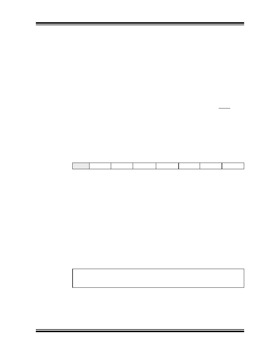
REGISTER 11-1:
T2CON: TIMER2 CONTROL REGISTER
U-0
R/W-0
—
TOUTPS3
TOUTPS2
TOUTPS1
TOUTPS0
TMR2ON
T2CKPS1
T2CKPS0
bit 7
bit 0
bit 7
Unimplemented: Read as '0'
bit 6-3
TOUTPS3:TOUTPS0: Timer2 Output Postscale Select bits
0000
= 1:1 Postscale
0001
= 1:2 Postscale
1111
= 1:16 Postscale
bit 2
TMR2ON: Timer2 On bit
1
= Timer2 is on
0
= Timer2 is off
bit 1-0
T2CKPS1:T2CKPS0: Timer2 Clock Prescale Select bits
00
= Prescaler is 1
01
= Prescaler is 4
1x
= Prescaler is 16
Legend:
R = Readable bit
W = Writable bit
U = Unimplemented bit, read as ‘0’
- n = Value at POR reset
’1’ = Bit is set
’0’ = Bit is cleared
x = Bit is unknown
发布紧急采购,3分钟左右您将得到回复。
相关PDF资料
PIC16C621A-40/SS
IC MCU OTP 1KX14 COMP 20SSOP
PIC16C622A-40/SS
IC MCU OTP 2KX14 COMP 20SSOP
PIC16CE623-30/SO
IC MCU OTP 512X14 EE COMP 18SOIC
PIC16CE624-30/SO
IC MCU OTP 1KX14 EE COMP 18SOIC
PIC16CE624-30/SS
IC MCU OTP 1KX14 EE COMP 20SSOP
PIC16CE623-30/SS
IC MCU OTP 512X14 EE COMP 20SSOP
PIC16CE624-30/P
IC MCU OTP 1KX14 EE COMP 18DIP
PIC16F722-I/SO
IC PIC MCU FLASH 2KX14 28-SOIC
相关代理商/技术参数
PIC18C442T-E/PT
功能描述:8位微控制器 -MCU 16KB 512 RAM 34I/O RoHS:否 制造商:Silicon Labs 核心:8051 处理器系列:C8051F39x 数据总线宽度:8 bit 最大时钟频率:50 MHz 程序存储器大小:16 KB 数据 RAM 大小:1 KB 片上 ADC:Yes 工作电源电压:1.8 V to 3.6 V 工作温度范围:- 40 C to + 105 C 封装 / 箱体:QFN-20 安装风格:SMD/SMT
PIC18C442T-I/L
功能描述:8位微控制器 -MCU 16KB 512 RAM 34I/O RoHS:否 制造商:Silicon Labs 核心:8051 处理器系列:C8051F39x 数据总线宽度:8 bit 最大时钟频率:50 MHz 程序存储器大小:16 KB 数据 RAM 大小:1 KB 片上 ADC:Yes 工作电源电压:1.8 V to 3.6 V 工作温度范围:- 40 C to + 105 C 封装 / 箱体:QFN-20 安装风格:SMD/SMT
PIC18C442T-I/PT
功能描述:8位微控制器 -MCU 16KB 512 RAM 34I/O RoHS:否 制造商:Silicon Labs 核心:8051 处理器系列:C8051F39x 数据总线宽度:8 bit 最大时钟频率:50 MHz 程序存储器大小:16 KB 数据 RAM 大小:1 KB 片上 ADC:Yes 工作电源电压:1.8 V to 3.6 V 工作温度范围:- 40 C to + 105 C 封装 / 箱体:QFN-20 安装风格:SMD/SMT
PIC18C452/JW
功能描述:8位微控制器 -MCU 32KB 1536 RAM 34I/O RoHS:否 制造商:Silicon Labs 核心:8051 处理器系列:C8051F39x 数据总线宽度:8 bit 最大时钟频率:50 MHz 程序存储器大小:16 KB 数据 RAM 大小:1 KB 片上 ADC:Yes 工作电源电压:1.8 V to 3.6 V 工作温度范围:- 40 C to + 105 C 封装 / 箱体:QFN-20 安装风格:SMD/SMT
PIC18C452-E/L
功能描述:8位微控制器 -MCU 32KB 1536 RAM 34I/O RoHS:否 制造商:Silicon Labs 核心:8051 处理器系列:C8051F39x 数据总线宽度:8 bit 最大时钟频率:50 MHz 程序存储器大小:16 KB 数据 RAM 大小:1 KB 片上 ADC:Yes 工作电源电压:1.8 V to 3.6 V 工作温度范围:- 40 C to + 105 C 封装 / 箱体:QFN-20 安装风格:SMD/SMT
PIC18C452-E/P
功能描述:8位微控制器 -MCU 32KB 1536 RAM 34I/O RoHS:否 制造商:Silicon Labs 核心:8051 处理器系列:C8051F39x 数据总线宽度:8 bit 最大时钟频率:50 MHz 程序存储器大小:16 KB 数据 RAM 大小:1 KB 片上 ADC:Yes 工作电源电压:1.8 V to 3.6 V 工作温度范围:- 40 C to + 105 C 封装 / 箱体:QFN-20 安装风格:SMD/SMT
PIC18C452-E/PT
功能描述:8位微控制器 -MCU 32KB 1536 RAM 34I/O RoHS:否 制造商:Silicon Labs 核心:8051 处理器系列:C8051F39x 数据总线宽度:8 bit 最大时钟频率:50 MHz 程序存储器大小:16 KB 数据 RAM 大小:1 KB 片上 ADC:Yes 工作电源电压:1.8 V to 3.6 V 工作温度范围:- 40 C to + 105 C 封装 / 箱体:QFN-20 安装风格:SMD/SMT
PIC18C452-I/L
功能描述:8位微控制器 -MCU 32KB 1536 RAM 34I/O RoHS:否 制造商:Silicon Labs 核心:8051 处理器系列:C8051F39x 数据总线宽度:8 bit 最大时钟频率:50 MHz 程序存储器大小:16 KB 数据 RAM 大小:1 KB 片上 ADC:Yes 工作电源电压:1.8 V to 3.6 V 工作温度范围:- 40 C to + 105 C 封装 / 箱体:QFN-20 安装风格:SMD/SMT